|
PULSE Research
Ultrafast Materials Science
Matter In Extreme Environments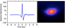
Fig. 1 (left) THz temporal profile. (right) Measured THz spatial profile (corresponding to a diffraction-limited spot of size ~500 microns)
a) We are currently investigating the response of materials to intense ultrafast electric fields, corresponding to quasi-half-cycle far infrared light pulses that turn on and then turn off in hundreds of femtoseconds. In initial experiments, we have used this to both probe and control carrier dynamics in semiconductors on ultrafast time-scales. We have observed THz-field-induced impact ionization, in which electrons and holes are accelerated in the applied field to energies sufficient to ionize and produce an avalanche of free carriers, occurring within the THz pulse. This may be viewed as THz self-phase modulation (in which the field is strong enough to modify the optical properties of the material as it propagates through the material) and opens up new windows into the field of nonlinear THz spectroscopy. Fig. 1 shows electro-optic sampling measurements of the THz temporal and spatial profile. Fig. 2 shows measurements of the change in carrier concentration dN/N induced by the ultrafast field (corresponding to far below band-gap photons) as a function of applied field. Also shown is a fit based on a simple impact ionization model. 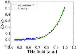
Fig. 2. Normalized change in carrier density as a function of THz applied field.
We are also investigating the response of ferroelectric materials to intense THz fields, attempting to measure the fundamental speed limits for how fast a ferroelectric can switch and the associated atomic-scale motion within the unit cell. b) We have completed analysis of a final set of experiments conducted at the Sub-Picosecond Pulse Source (SPPS) representing the first ever femtosecond time-resolution x-ray diffuse scattering measurements. In these experiments, the nucleation of nanoscale voids near the surface of an ablating semiconductor (InSb) were observed as a function of time in the small angle scattering regime. These measurements are important for understanding how materials evolve under extremes of temperature and pressure. Fig. 3. shows raw data along side MD simulations of the observed effects near the surface, in good agreement with our experimental data. 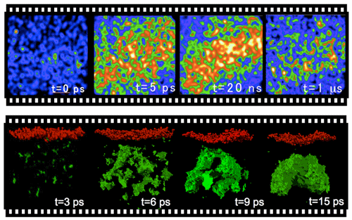
Fig. 3 (top) Raw snapshots of the x-ray scattering from an optically-excited semiconductor near the ablation threshold as a function of time. (bottom) MD simulations showing the build-up of nanoscale voids (green) beneath the surface, the first steps in the ablation process.

|